HI-8596PCI
HI-8596 Series Line Driver
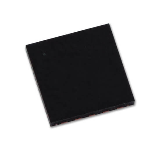
The HI-8596 bus interface product is a silicon gate CMOS device designed as a line driver in accordance with the ARINC 429 bus specifications. The part includes a dual polarity voltage doubler, allowing it to operate from a single +3.3V supply using only four external capacitors. The part also features high-impedance outputs (tri-state) when both data inputs are taken high, allowing multiple line drivers to be connected to a common bus. Logic inputs feature built-in 4KV ESD input protection (HBM) as well as 5V or 3.3V logic level compatibility. 37.5 Ohm or 5 Ohm resistors in series with each ARINC output are available to allow the use of external resistors for lightning protection. The HI-8596 line driver is intended for use where logic signals must be converted to ARINC 429 levels such as when using an FPGA or the HI-3586 ARINC 429 protocol IC. The part is available in Industrial -40?C to +85?C, or Extended, -55?C to +125?C temperature ranges. Optional burn-in is available on the extended temperature range.
Key Features
- +3.3V Single Rail Supply Voltage
- All ARINC voltage levels generated on-chip
- Digitally selectable rise and fall times
- Tri-state Outputs
- 5 Ohm or 37.5 Ohm output resistance
- Built-in 4,000V minimum ESD Protection of Logic Inputs
- 5V or 3.3V Logic Level Compatibility
- Plastic 16-pin SOIC & QFN packages available
- Lead-free / RoHS Compliant options available
- Industrial & Extended Temperature Ranges
- Burn-in Available
Need help selecting the right solution?
Our technical specialists can help you choose the right product, answer technical questions and provide a quotation.
Technical Specifications
| Temperature Range | -40°C to +85°C |
|---|---|
| RoHS | No |
| Applications |
|
| Burn In | No |
| Flow | I |
| Moisture Sensitivity Level | 3 |
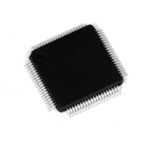
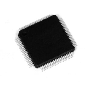
| Package Description | 16 Pin 4mm x 4mm Plastic Chip Scale (QFN) |
| Theta JA C W | 55.1 |
| Theta JB C W | 38.5 |
Downloads
| Datasheet | Click to view Datasheet (PDF) |
|---|